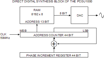
Here is the block diagram of the DDS block of the PCGU1000:

To the RAM of 8192 bytes is stored the look-up table for one cycle of the waveform.
A constant value, the phase increment, is added to the address counter with each 50MHz clock cycle. If the phase increment is large, the address counter will step quickly through the look-up table and thus generate a high frequency wave. If the phase increment is small, the address counter will take many more steps, accordingly generating a slower waveform.
The 13 highest bits of the address counter are connected to the address lines of the RAM.
If the phase increment is very low then several clock pulses are needed to increment the RAM address.
To get high frequency out the phase increment value will be high and the RAM address is incremented in big steps. For instance if 2MHz frequency is to output, there are needed only 25 pulses from the 50MHz clock to go through the whole RAM address space. The RAM address will increment 8192/25 = 327.68 address locations on each 50MHz clock cycle.
Here is the formula to calculate the RAM address (13 MSB of the address counter) increment:
RAM ADDRESS INCREMENT = 8192 * (output frequency) / 50MHz
Example:
We want 10kHz output
RAM ADDRESS INCREMENT = 8192 * 10kHz / 50MHz = 1.6384
Here we see that to get 10kHz out the RAM address is increment this amount 1.6384 on every 50MHz clock. This kind of decimal number as an address increment is possible using the 44 bits long phase increment register.
(The value to the phase increment register can be calculated following way:
PHASE INCREMENT = 2^44* 10kHz / 50MHz = 3518437209 )
At 10kHz the time for each RAM address location is 20ns/1.6384 = 12.20703ns
Now we like to generate the custom waveform file for five 1us pulses with 0.1us pause between each pulse.
To get 1us pulse, the number of samples is 1us/12.20703ns = 81.92 samples
To get 0.1us pause the number of samples is 0.1us/12.20703ns = 8.192 samples
To get five such pulses, we have to write the following LIB file:
-1.0(7742)
1.0(82)
(0)
-1.0 (8)
(0)
1.0(82)
(0)
-1.0 (8)
(0)
1.0(82)
(0)
-1.0 (8)
(0)
1.0(82)
(0)
-1.0 (8)
(0)
1.0(82)
(0)
-1.0 (8)
The actual values are:
Pulse width = 82 * 12.20703ns = 1.00097us
Pause width = 8 * 12.20703ns = 0.976us
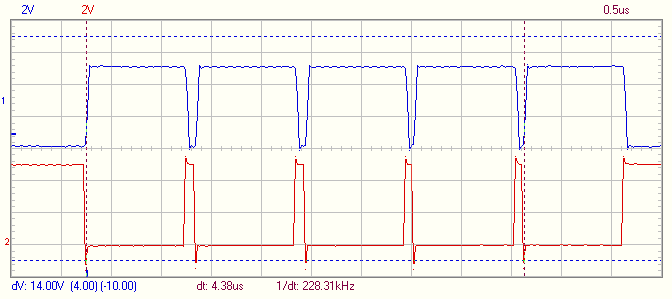
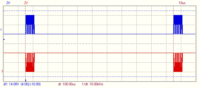
Here is the resulting waveform:


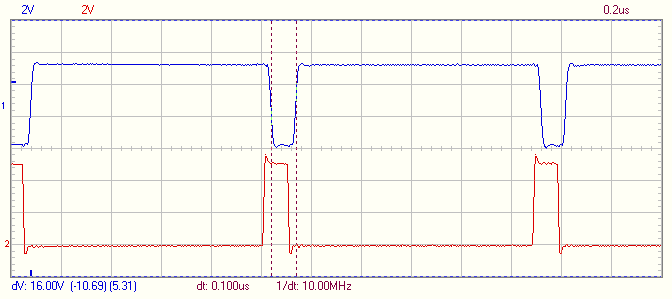
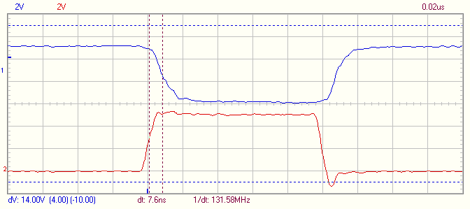
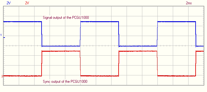
[quote]1. How did you get simultaneously two paraphase signals? It was just remembering function on oscilloscope or you used mentioned FPGA decision?[/quote]I made a minor FPGA modification to invert the sync signal.
[quote]1.1 On your plot shift between paraphase signals is about 0.2us/10=20ns, i.e. good for me, 'cause I need it less than 50ns. Will FPGA modification be able to get this shift not more, than on your plot?[/quote]Yes, the sync signal can be delayed in the FPGA.
[quote]2. I thought FPGA is scheme with Atmel or something like that, but you mentioned “modified file”. What did you mean: some modified file for PCLab 2000, scheme with Atmel or something else?[/quote]The file to be modified is the pcgu1000.bit in the PCLab2000SE folder. You just replace the existing file with the new one.
