Very surprised to receive a ‘topic reply notification’ email on a forum I had forgotten I had signed up to, never mind not remembering posting too! Anyhow, I’m quite happy to have a go at describing the Mk152 oscillator’s operation!
The oscillator is formed by C2, R1, R2, C1, IC1E, IC1D, IC1A, D1 & R3, and it is made voltage-controlled by R4/C3 and the effect of D1. But first let us step back a little, and consider the more basic oscillator formed by disconnecting R4 and removing D1 from the circuit by shorting it out. Within this set-up, components R1, R2, C1, IC1E, IC1D form a Schmitt trigger, and first of all let’s deal with C1: because of the double inversion through IC1E & IC1D, output pin 8 has essentially the same phase as input pin 11 - this has the potential for high-frequency oscillations to arise, and it seems C1 has been added to provide a little extra phase lag in order to prevent this from happening. In any case, C1 charges/discharges very quickly through output pin 8, as the effective resistance through whichever output transistor of the inverter is on (either up to rail, or down to ground) will be of the order of a few hundred ohms at most. Certainly simulations of the circuit run well enough without it, so from now we’ll ignore C1!
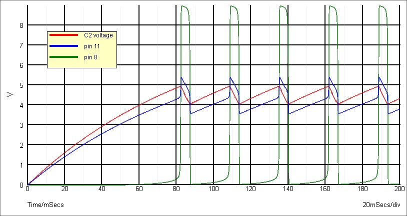
So now back to R1/R2/IC1E/IC1D: if the input voltage applied at R1 is low, and the output at pin 8/R2 is low, the voltage at pin 11 due to potential divider R1/R2 is also low, so output pin 10/input 9 is high, and pin 8 is low, as assumed, and all is good. If the voltage at R1 increases, so does that at pin 11; eventually the voltage there will reach the threshold, about mid-rail, above which the inverter output will flip to the other state; so pin 10/pin 9 go low, and pin 8 goes high; as 8 is connected to R2, the effect of this is to further increase the voltage at pin 11, thus positively reinforcing the change of state. In order to flip back again, the voltage at R1 has to fall substantially, until the voltage at 11 again nears the threshold voltage, where the reverse action happens, pins 10/9 go back high, pin 8 goes low again. The amount of this hysteresis is determined by the ratio of R1 to R2, and is about 1V.
Thus the oscillator action is as follows: suppose C2 voltage is low enough that the first inverter output, pin 10 (& 9) is high; the second, pin 8 (& 1) is low, and the third, pin 2 is high. C2 is then being charged from high pin 2 through R3 (remember we’ve shorted the diode), and eventually reaches the point where the first inverter output, pin 10 flips state to low, quickly followed by the others, pin 8 high, pin 2 low. Now C2 discharges through R3, and when it discharges far enough, all the outputs flip again, and so the oscillator (really ‘multivibrator’) action proceeds.
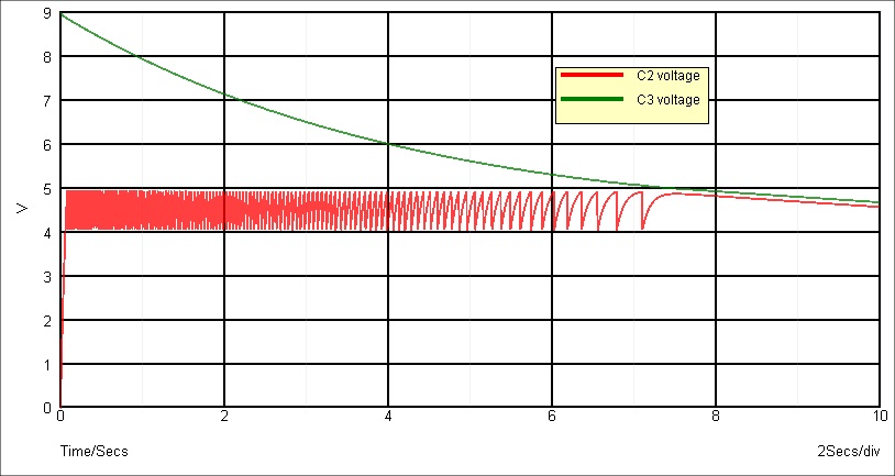
Now let’s add R4 (& C3) and D1 back in. The diode D1 prevents C2 from charging from pin 2 through R3; instead it is charged from C3 via R4. Before SW1 is closed, R5 pulls the inverter input pins 13/3/5 low, so all outputs are high, and thus none of the LEDs connected to IC2 can light, so the whole device appears ‘off’. When SW1 is closed, capacitor C3 rapidly charges to the rail, and C2 starts to charge through R4. When C2 reaches approximately 0.5V above mid-rail, the oscillator bursts into life, and it starts clocking IC2; as inverter inputs 13/3/5 are high, the outputs 12/4/6 are low, and so the LEDs can light in turn. Even after SW1 is opened, there is enough charge on C3 to continue charging C2 via R4, but as C3 charge falls away, the re-charge time for C2 gets longer and longer, and so the oscillator starts to slow down (C2 discharges through R3 and D1 at a fairly constant rate throughout). Eventually C3 drops to around mid-rail, and it can no longer charge C2 high enough for the oscillator to continue running, and the whole thing stops.
The two images show simulation traces starting with C3 charged to 9V (i.e. SW1 having been pressed and released), and C2 starting at zero volts. One shows C2 voltage increasing until the oscillator starts, and for a few cycles after that, along with pins 11 & 8; the other shows C2 and the decreasing voltage on C3 as it discharges, eventually dropping to the point where C2 cannot get high enough for oscillations to continue, and so the whole thing stops.