Laser/milling CNC mod

Newbie here - just finished assembling my K8600.

Has anyone modified the Nano with either a laser or milling head? I’m interested in using the printer as part of a rapid prototyping process to create PCBs. Either a laser etch and photo/chemical process or a physical milling process would be great. If anyone has any guidance, suggestions or designs I’d be super interested.

Thanks

Mr Q

With all the dust produced by a CNC I’m not sure if that’s a good idea. The mainboard and other components are under the print bed are will be exposed to this hostile environment. Also I found (Chinese?) mini CNC/laser engravers that are very cheap nowadays. Here is an example: https://www.amazon.co.uk/Qiilu-Engraving-Wireless-Bluetooth-Engraver/dp/B072K24LGL?SubscriptionId=AKIAILSHYYTFIVPWUY6Q&tag=duc08-21&linkCode=xm2&camp=2025&creative=165953&creativeASIN=B072K24LGL.

1 Like

That’s a good point.

Well I’ve already made a lot of progress towards modding the printer so I’ll persevere but I’ll consider ways to mitigate the dust and debris problem. A vacuum attachment perhaps. vacuum pump

I’ve redesigned the hot end bracket to accept proper linear bearings instead of brass bushes. I bought the bearings on tatBay from China and could only get 12mm long bearings. The clips on the bracket are 8mm. I’m also designing a printed bracket that clips into the same “U” shaped slot as the hot end assembly to accept drilling and milling mechanism. This will have ball bearings to support a carbon fibre shaft holding the chuck and a flexible drive shaft driven from a motor mounted under the control board. There’s just enough space to mount this in a printed clip. It will drive more carbon fibre rods through a printed gearbox with a couple of bevel gears to the top of the rear of the printer. A hex drive will connect this to the drill head via the flexible drive.

Back to your point, drilling 0.5mm holes in PCBs will not create a lot of dust. Milling will create considerably more so perhaps I’ll abandon this idea. I was already toying with two potential methods of making the PCBs. One was milling away the 0.04mm copper surface around the tracks. The other is spray painting the surface then scribing the track layout (inverted) and using a chemical etch process to dissolve the exposed copper.

I can easily make a spring loaded scriber in a custom printed bracket to achieve this. Or perhaps simply use a ball head engraving bit in the drill chuck.

Another option is a laser to etch photosensitive coating on the copper clad board.

Another option is fitting a laser and etching photo sensitive chemical mask.

Interesting read. If you continue with your project it would be worthwhile to see your progress. Do you have a project page for this?

No this project is partly secondary to my work, at least not a priority so I haven’t had time to think about documenting it. Also I’m new to this forum and to 3D printing in general - just feeling my way. I’ll have a think about documenting it and, for sure, when I have parts that work (or don’t work for whatever reason) then I’ll post photographs.

Thanks for your interest Eric.

I know this is an old topic, but is there still interest for this kind of mod?
I am currently experimenting with laser etching PCB’s, using the Nano and a cheap Chinese near-UV laser. My hope is to get down to reliably reproducing 6-8 mil traces. I am not there yet, but I am getting quite close:

1 Like

Very nice!

I am definitely interested to see more about this project, both the hardware modifications and how you process the layout files into gcode.

Please wear proper eye protection!

Very well. I will write something up, once I remember where I have the files for the laser adaptor. In the mean time, here is a little teaser from my latest attempt (which is being etched right now):

https://www.youtube.com/watch?v=eHkhpDfUjdo

2 Likes

Wow, that etches a lot faster than I would have expected. What is the power rating and wavelength of your laser?

That is really cool.

The laser is a cheap Chinese 405 nm 500 mW one, but I run it at less than 10% power.
I only use the laser for exposing the photo resist, not cutting through it. The PCB needs to go through the usual chemical developing and etching processes afterwards.

I printed a couple of 3D parts in order to mount the laser on the printer. The files are here, if anyone wants to duplicate my setup:
Vertex Nano laser adaptor files
The 3D printhead is removed, and the laser adaptor inserted instead.

The laser also needs to be controlled by the printer. For this I have followed the instructions from Niels Jallings blog: http://oz9ny.blogspot.com/2017/06/modifying-firmware-for-fan.html
Only, I connect my laser to the printer instead of a fan. This firmware modification allows me to control the laser power (from 0 to 255) with the M106 g-code.

I think that is what I have on the hardware side of things. Next I’ll talk about how I create the g-code file for this.

Oh, by the way: The PCB from the video above turned out great. Not pixel perfect, but definately good enough for being usable:

1 Like

Now for the g-code generation…

I use Eagle as my PCB layout program, and pcb-gcode (a kind of “plugin” to Eagle) to generate the g-code file, though the result needs some post processing. I have older versions of Eagle (5.12.0) and pcb-gcode (3.5.2.11), so things may need to be fixed if using newer versions. You have been warned :wink:

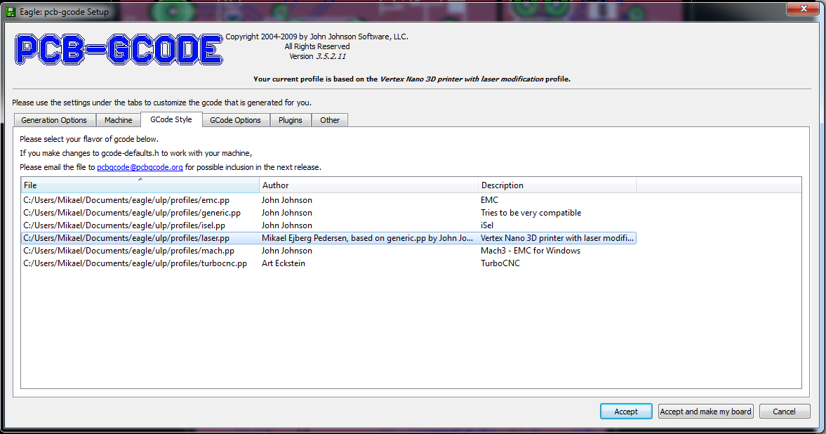
First, I have made a new profile for pcb-gcode, that will need to be placed among the existing profiles:
pcb-gcode Vertex Nano machine profile
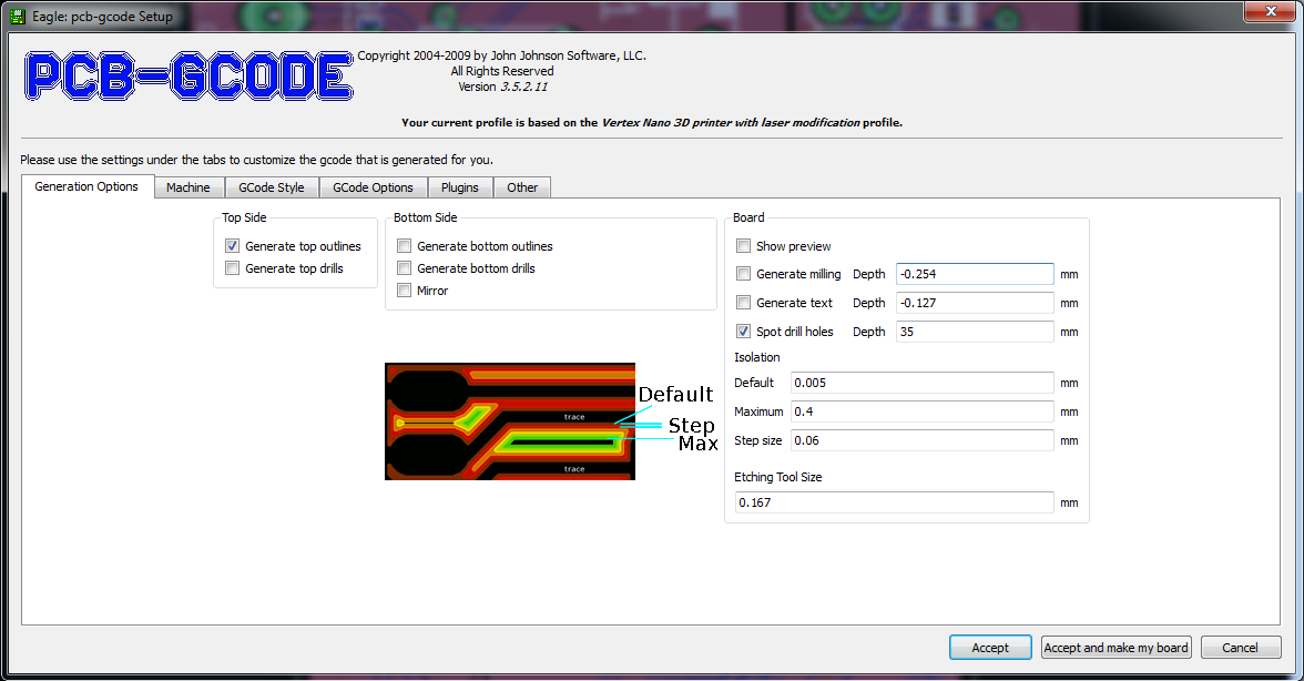
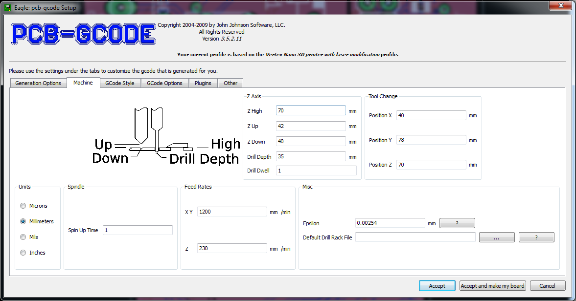
Then I use these settings in pcb-gcode:


Note the settings for “Z Up”, “Z Down” and “Drill Depth”. The numbers mean nothing, but they need to be different from one another, as we are going to use them in a moment.
Now click “Accept and make my board”, and Eagle will generate a .ngc file.

This .ngc file is g-code, but we can’t use it just yet (for that, I still need to do some work on the pcb-gcode machine profile).
Now open the .ngc file in an editor, one with a search and replace function. I prefer Notepad++
First, find a line near the top containing:
G00 X0.0000 Y0.0000 F9000
Change it to:
G00 X0.0000 Y0.0000 Z2.0000 F9000
(just add Z2.0000 in there). My laser is focused for use at 2 mm height.

Next, use search/replace to find all lines with:
G01 Z40.0000 F230.00
and replace them with:
M106 S25
The Z40 indicates that this is a “Z down” command (from the pcb-gcode settings above). This is replaced with the gcode M106 S25 that turns on the laser at 10% power.

Again search/replace all lines from:
G00 Z42.0000 F9000
to:
M107
This is “Z Up”, and M107 turns the laser off.

Finally do one more search/replace:
G01 Z35.0000 F230.00
shall be:
M106 S25
G04 P100
Yes, two lines. In Notepad++ this can be entered as “M106 S25\nG04 P100” in the replace dialog.
This makes the drill spot marks.

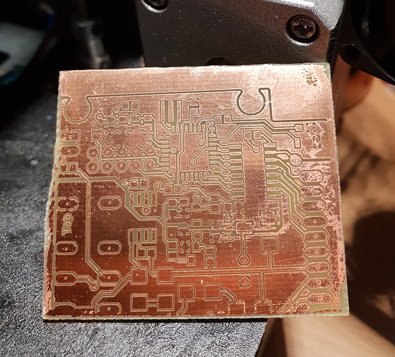
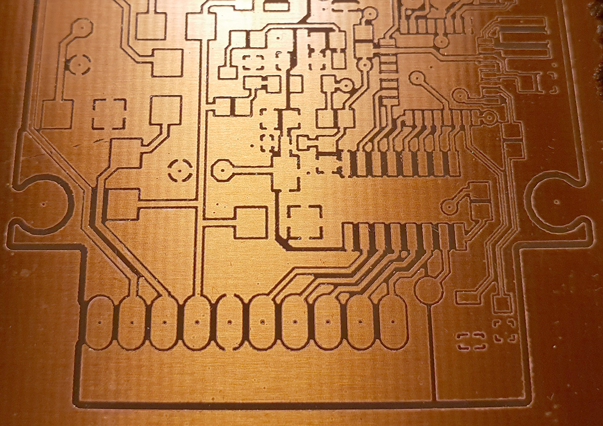
That is all. Save the modified file to a SD card, and put a photosensitive PCB in the Vertex Nano.

1 Like

Thank you for the detailed write-up!

There are a lot of steps, but you’ve laid it out nicely. The gcode post-processing you describe could be automated, and it looks easy to adapt this to any model of printer.

My hope is to get pcb-gcode to write a fully functional file, without the need for post-processing at all. Some day… Eventually… :stuck_out_tongue:
And you are right, there is no Vertex Nano specific in this process, so any printer will do. As long as it has an output for a laser, that can be controlled by a g-code command.

For debugging, the generated g-code can be viewed online with NC Viewer:
https://ncviewer.com/
That is handy for a sanity check before committing to exposing a PCB.

That day is apparently today. I have tinkered some more with the pcb-gcode profile, and now all the manual search-replace isn’t needed anymore. Get the new profile here:
Pcb-gcode laser exposing machine profile v2

The magic numbers in “Z High”, “Z Up” and “Z Down” aren’t needed anymore.
Instead some parameters are used this way now:
“Z High”: This is where the Z axis goes to when the exposure is over. Set this high to be able to get the PCB out.
“Z Up”: Not used.
“Z Down”: The Z height where the laser is in focus on the PCB. I use 2 mm.
“Drill Depth”: This is used for setting the laser intensity. Values between 1-255, where 255 is max power. I use 25 on my 500mW laser.
“Drill Dwell”: Exposure time at spot drill holes, in ms. I use 100.
“X Y Feed Rate”: The speed at which the laser moves when drawing lines. I use 1200 mm/min.

One thing I haven’t tried yet, is double-sided boards. I suspect that trying to create a file for the bottom side will result in negative X coordinates, that 3D printers don’t handle well.

1 Like