I have assembled the EDU09 oscilloscoop, but the calibration failed. In the calibration log I found:
Calibration results:
CH1 offset at 5V/div : 59 FAIL
CH1 offset at 1V/div : -201 FAIL
CH1 Y-position low 201
CH1 Y-position mid 201
CH1 Y-position high 201
I cannot find an explanation about the log file and have no clue in which direction I should look for loose contacts or mis-placements of components. Can someone give me a hint?
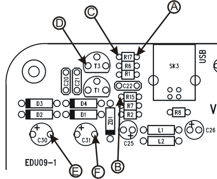
I have checked T1, T2, and T3. T1 and T3 are both located near the USB connector. T1 is BC337-16, T3 is BC327-25. The T3 is located near the relay switch and is a BC337-16.
Are there any other pointers?
How does the calibration work? What and in which order are things checked by the program?
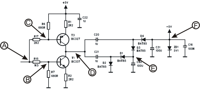
As far as I’ve seen, the calibration is just for the DC offset. Your values indicate a very big dc offset, that is why something could have been wrong with T1/T3 because they are part of the charge pump for negative voltage.
Please check the voltage over the zener diode ZD1.
There should be about 5V.
If not:
Check the right polarity of ZD1 and all other diodes.
Check all the components of the charge pump circuit around T1 and T3 near the USB connector.
I’ve checked all the diodes and all were OK. However I had only a few milivolts over the zener diode. I decided to solder it out, but I wrecked the zener diode. I have ordered a new 5.1V zenerdiode. So I have to wait until that one comes in. I have however a question about the zener diode. The drawing in the assemble guide shows that the kathode should be on the side where the thick line is drawn. It was assembled that way. But is that correct?
[quote]However I had only a few milivolts over the zener diode.[/quote]Most probably the charge pump that should generate the -5V is not working.
[quote]The drawing in the assemble guide shows that the kathode should be on the side where the thick line is drawn. It was assembled that way. But is that correct?[/quote]That is correct.
Thanks for the drawings. I have soldered the zener diode in again and checked the program if it could calibrate it now. The calibration failed, but with another result:
Calibration results:
CH1 offset at 5V/div : 59 FAIL
CH1 offset at 1V/div : -201 FAIL
CH1 Y-position low 197
CH1 Y-position mid 197
CH1 Y-position high 197
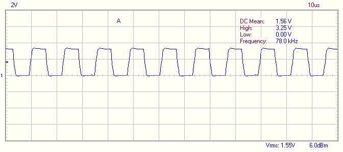
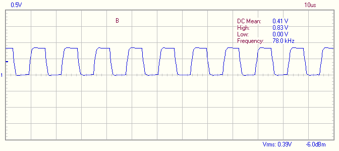
I have measured the points as pointed out by VEL255 and my results are:
A = 1.66 V
B = 0.37 V
C = 4.49 V
D = 2.60 V
E = -4.97 V
F = 0.75 V
Points A, B and C looks alright. Point D is somewhat below and E and F are far way out.
After studying the schema and the tips of VEL255 I have again measured the charge pump and I see on diode D1 a -2.4 V, while on point E a -4.97 volts is measured. To my humble opinion the capacitor C20 or de diode D3 must be defect. I don’t have the parts, so I have to order them again. How can I found out which component is the culprit? Am I on the right track?
It seems the diode D3 or D4 is defective.
Please check the anode of diode D4 has connection to ZD1.
Please check the diodes D3 and D4 and the connections.
Last weekend I assembled one myself and ran into the same calibration log error you did.
While looking for a solution I stumbled on Your question.
after a good night sleep I discovered where the problem was
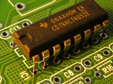
In my case I placed the 8 pin IC the wrong way around because of the missing notch.
After turning it around the calibration was successful and the unit worked like a charm.
I don’t know if it is the solution for You but it worth a try I think
the dot on the ic should be on the side of the 2 cables
I have replaced the diodes D3 and D4 and also capacitor C20, but the same problem. The CD74HCT4052E has a dot and a notch, so I decided to see the dot as the pin 1 and the calibration now shows:
Calibration results:
CH1 offset at 5V/div : 161 OK
CH1 offset at 1V/div : 201 FAIL
CH1 Y-position low 0
CH1 Y-position mid 0
CH1 Y-position high 0
So it looks like I’m one step further, however I found the CD74HCT4052E getting hot.
Now I need to know how the CD74HCT4052E should be placed and how the CH1 offset at 1V/div :201 FAIL could be resolved.
I have bought a new EDU09 kit at Conrad and have assembled it today. From the spot the calibration went OK. So I have a working kit and a non-working kit. But now I have the chance to compare them and try to find out where the problem is. The problem is still not solved. but when the weather get worse I will sit down and find it, I hope. I’ll keep you posted when I find the problem. Thanks so far for the help.
Thank you for the feedback.
I’m glad to see you had better success with the second EDU09 kit!
It is also interesting to know what is the cause of the calibration problem with the first EDU09.
I have a second working EDU-09. For me, as a newbie electronics, that’s a real victory. But what was the real cause of the failure in the first place? To be honest I’m not 100% sure, but I suspect the PCB had a missing trace. What have I done? First of all I replaced all diodes (D1, D2, D3 and D4) and the zener diode (ZD1). Then I also replaced the ceramic capacitors (C20 and C21) and the electrolytic capacitors (C30 and C31). But the calibration still failed. Then I decided to desolder all above components and to put them on a breadboard. I made connections from the collectors of the transistors (T1 and T3) to the breadboard and connected the ground. I then connected the output of the zener diode to the hole above the C19 capacitor. Plugged in the USB cable and started the program and calibrated the EDU09. IT WORKED!!. Later on I have soldered the parts on a piece of test board and have added that board to the EDU09 with the connections as described above. It doesn’t look pretty, but it works and I can use it. The EDU09 works like a charm. All other functions work also for me. So if you aks me where the problem was I would think that on the PCB there was no connection between C20 and C21 capacitors. After desoldering a few times you can see that the hole pads get really worse and therefore I cannot prove it anymore. Anyway thanks for all the help.